utility menu


Quality Commitment
As one of the largest back-end toll processing company in Korea.

Reliability Capability
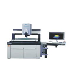
FuRex 는 정확하고 정밀한 분석을 위해 다양한 Testing 장비를 구비하고 있습니다.
-
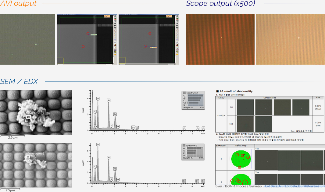
Visual Inspection
-
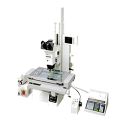
Measuring micro
-
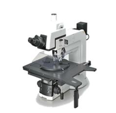
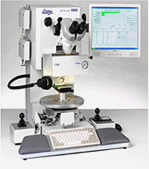
High power scope
-
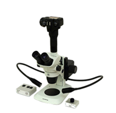
Low power scope
-
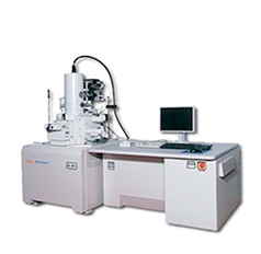
FE – SEM / EDX
-
-
Performance
Test-
Vibration
-
Drop
-
Roughness
-
Thickness
-
-
Reliability
Test-
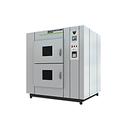
Thermal shock
-
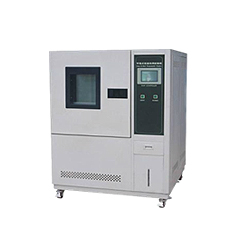
Temp& Humidity
-
As you see, these are the examples of the scope of our reporting.
Having such feedback process we strive to find the issues as early as possible, respond to the issues as early as possible.
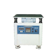
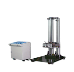
Reliability
-
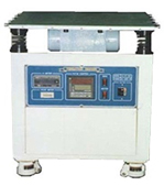
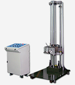
- Vibration Tester
- Green Science
- Vibration 10~100HZ
-
- Drop Tester
- ODM
- Max 1.7M
-
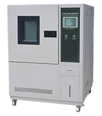
- Temp
& Humidity chamber - SJ-109 (So Jung)
- -20℃ ~ +120℃ / 30 ~ 98%RH
- Temp
-
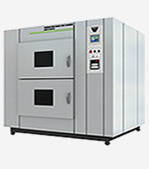
- Thermal
Shock Chamber - SJ-TS2 (So Jung)
- Temp range: -70℃ ~ +180℃
- Thermal
-
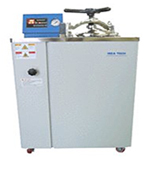
- Pressure
Cooker Tester - PCT-48 (이레테크)
- Temp range: 80℃ ~ 130℃
- Pressure
-
- Wire Bond Tester
- Dage4000 (Nordson)
- Wire bond pull,
ball shear, die shear
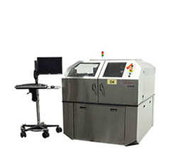
Failure Analysis
Thermal Field Emission-SEM
(주사전자현미경)
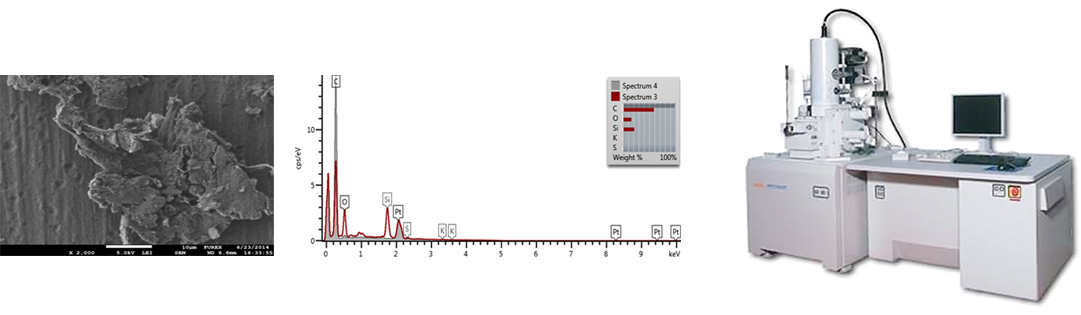
- Model: JSM7610 (JEOL)
- Resolution : 1.0nm at 15kV, 1.5nm at 1kV
- Magnification: X25 to X1,000,000
- Accelerating Voltage : 0.1kV to 30kV
전자 빔이 표면에 집중되어 1차 전자만 굴절되고 표면에서 발생된 2차전자를 수집하여 그 신호들을 형상화 시키는 현미경으로서 시료 표면의 정보를 얻을 수 있습니다.
낮은 가속전압에서도 시편 관찰이 용이하여 전자 빔에 의한 시료의 손상을 최소화 할 수 있으며,
ESD 가 부착되어 있어 시편의 성분과 표면성분에 관한 연구를 수행할 수 있습니다.
![]()
Address : 283, Sandan-ro, Danwon-gu, Ansan-si, Gyeonggi-do, Republic of Korea
Tel: 031-428-2500 Fax : 031-454-1172
COPYRIGHT(C) 2017 FuRex